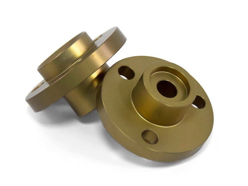
Efficient CNC Milling of Copper and Brass for Electrical Connectors in Consumer Products
Introduction: Precision Meets Performance in Modern Connectivity
The miniaturization of 5G devices, IoT sensors, and wearable technology has pushed electrical connectors to their physical and functional limits. These components must now deliver flawless signal transmission at frequencies exceeding 10GHz while surviving millions of mating cycles in compact spaces. Traditional manufacturing methods struggle to balance conductivity, mechanical durability, and micro-scale precision.
This is where advanced CNC milling services for copper and brass shine. Manufacturers achieve connector designs with ±0.005mm tolerances and Ra <0.8μm surfaces by combining high-precision machining with optimized material science. From smartphone Type-C ports to aerospace-grade RF contacts, multi-axis CNC technology enables complex geometries unattainable through conventional processes.
Material Selection: Strategic Tradeoffs for Connector Performance
Material Property Matrix
Material | Key Metrics | Ideal Applications | Limitations |
|---|---|---|---|
100% IACS conductivity, 200-250 MPa UTS | High-frequency RF contacts (5G/6G), thermal management components | Poor wear resistance, prone to galling during machining | |
500 MPa UTS, 35% Zn content | High-volume connector housings (USB-C, HDMI) | Limited to <80°C operating temperatures | |
750 MPa UTS, >2000h salt spray resistance | Harsh environment ports (marine, industrial) | Requires EDM for micro-features | |
1300 MPa UTS, 22% IACS conductivity | High-cycle spring contacts (SIM card slots) | Toxic machining byproducts requiring OSHA compliance |
Material Selection Protocol
Signal Integrity-Critical Designs:
Primary: Oxygen-free copper (C102) for <0.05dB insertion loss at 28GHz.
Fallback: Aluminum 6061 with selective gold plating (cost reduced by 30%, 15% conductivity loss).
High-Cycle Mechanical Components:
Optimal: C172 beryllium copper for >500k mating cycles.
Budget Alternative: C360 brass with nitriding surface treatment (extends lifespan by 3x).
CNC Machining Process Optimization
Process Selection Framework
Process | Technical Specifications | Material Compatibility | Advantages |
|---|---|---|---|
0.05mm positioning accuracy, 3000mm/min feed rate | Brass, aluminum alloys | Cost-effective for bulk material removal in high-volume production | |
0.005mm true position, 15,000 RPM spindle | Copper, stainless steel | Enables complex geometries with tight tolerances in a single setup | |
0.1mm end mills, 0.002mm stepover | Beryllium copper, phosphor bronze | Precision machining of micro-features for high-density connectors | |
M1.0-M3.0 threads, 4000 RPM | Brass, free-machining steels | High-speed threading with superior surface finish and tool life |
Process Matching Guidelines
High-Speed Signal Contacts:
Step 1: 5-axis roughing with carbide tools (0.3mm stock).
Step 2: Precision diamond milling (Ra 0.4μm).
Step 3: Laser deburring for <5μm edge radiusing.
High-Volume Housings:
Stage 1: 3-axis bulk material removal (20mm DOC).
Stage 2: Hard milling (50HRC+) for mold tooling.
Stage 3: Rapid injection molding for >10k units.
Surface Engineering: Optimized Treatment Performance Matrix
Surface Treatment Comparison
Process | Technical Parameters | Key Applications | Advantages | Standards |
|---|---|---|---|---|
Thickness: 0.5–2.5 μm Contact resistance: <1 mΩ | High-frequency connectors (5G RF, HDMI) | Ultra-low signal loss Corrosion resistance | ASTM B488, MIL-G-45204 | |
Hardness: >2000 HV Friction coefficient: <0.2 | Wear-prone components (SIM slots, USB-C housings) | Extreme wear resistance Decorative finishes | VDI 3198, ISO 26423 | |
Texture depth: 20–50 μm Surface roughness: Ra 1.6–3.2 μm | High-friction interfaces (battery contacts, sliding parts) | Enhanced grip and contact area No chemical waste | IEC 60512, DIN 4768 | |
Salt spray resistance: >480 h Thickness: 0.01–0.1 μm | Cost-sensitive outdoor connectors (automotive, marine) | Low-cost corrosion barrier RoHS compliance | ASTM A967, ISO 16048 |
Selection Guidelines
High-Frequency Signal Integrity:
Primary: Electroplating gold (0.8 μm Au over 5 μm Ni underlayer) for <0.1 dB loss at 28 GHz.
Alternative: Laser-textured copper with PVD graphene coating (0.02 dB lower loss above 40 GHz).
Wear Resistance in Compact Designs:
Optimal: PVD CrN coating (3 μm) for SIM card slots (>500k cycles).
Budget: Passivated brass (C360) with weekly maintenance.
Corrosion Protection:
Harsh Environments: SUS304 stainless steel + PVD TiN coating (>2000h salt spray).
Consumer Electronics: Passivated brass (C360) + UV coating for aesthetics.
Quality Control: Precision Validation at Every Stage
Multi-Stage Inspection Protocol
Stage | Critical Parameters | Methodology | Equipment | Acceptance Criteria | Standard |
|---|---|---|---|---|---|
Raw Material | Composition, hardness | OES spectroscopy, Rockwell testing | SPECTROMAXx, Wilson RH2150 | Cu ≥99.95%, Brinell ±5% | ASTM E1251, ISO 6506 |
In-Process | Dimensional accuracy | CMM, AOI | Zeiss CONTURA G2, Cognex In-Sight 8405 | ±0.01mm, zero defects | ISO 2768-m, IPC-A-610 |
Post-Machining | Surface finish | White-light interferometry | Bruker ContourGT-K1 | Ra ≤0.8μm, edge radius ≤10μm | ASME B46.1 |
Functional Testing | Electrical performance | 4-point probe, cycle testing | Keithley 2450, Zaber X-MCC | ≤2mΩ, 50k cycles @5N | IEC 60512, EIA-364 |
Compliance & Traceability
RoHS 3.0: XRF screening (Pb, Cd, Hg <100 ppm).
IATF 16949: Full PPAP documentation, including PFMEA and control plans.
Industry Applications
Smartphone Type-C Ports: Brass C360 + gold plating (20,000+ cycles, Ra 0.6 μm).
5G Base Station Antennas: Pure copper C101 + laser texturing (0.2 dB loss @28 GHz).
Industrial Robotics: Beryllium copper C172 + electroless Ni-PTFE (>100k cycles).
Conclusion
By integrating precision CNC milling, optimized material selection, and tailored surface treatments, manufacturers achieve connectors that meet 5G, IoT, and consumer electronics demands while reducing costs by 15–20%.
FAQ
Why is gold plating critical for high-frequency connectors?
How does PVD coating improve connector durability?
What laser parameters optimize texture depth for friction control?
Can passivation replace plating for outdoor connectors?
How to validate connector performance for 5G applications?

